Wafer Test Process
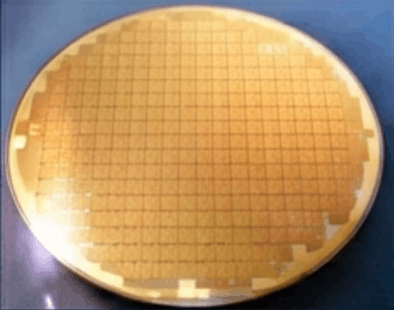
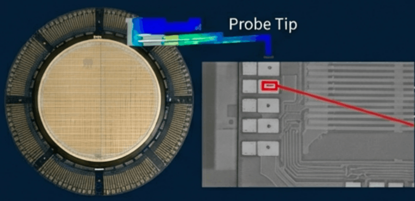
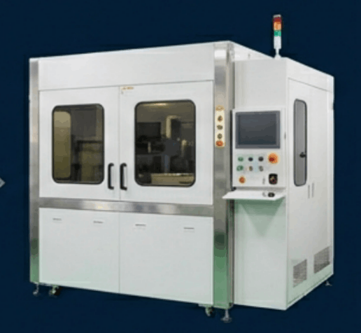
Prestandard: A core inspection device that identifies good and defective products by sending electrical signals to each chip on the wafer.
(A core inspection device that identifies good and defective products by sending electrical signals to each chip on the wafer.)
Technical Precision: MLC Type Probe Card Structure
Multi-layer ceramic structure design for complex signal processing
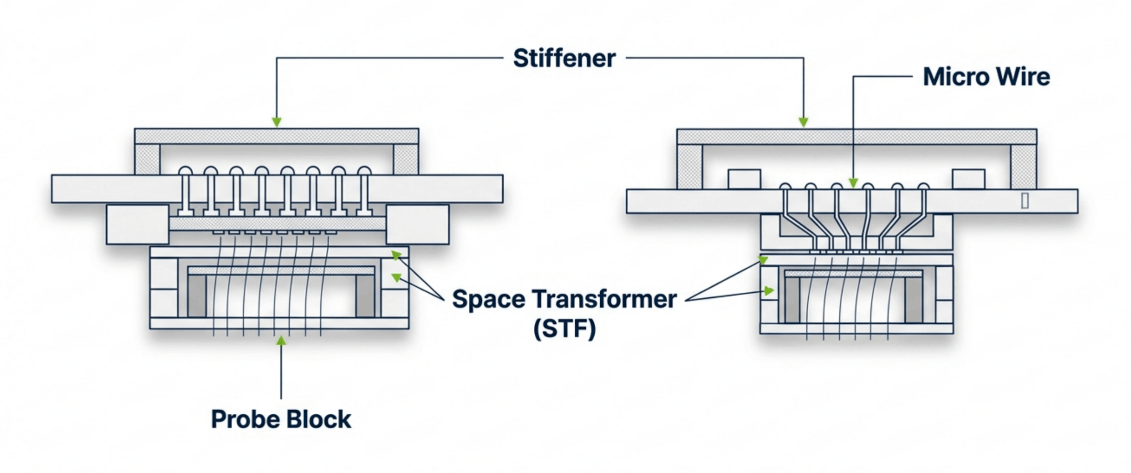
Space Transformer (STF)
Innovative Memory MEMS Probe Card Structure
Optimized part application through structure analysis and thermal deformation testing
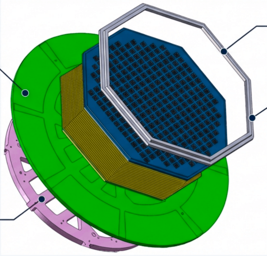
Ultra-fine MEMS Probe Technology Applied
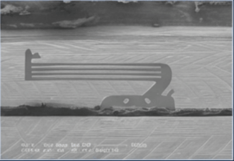
Overwhelming Spec Difference
Cantilever vs MEMS Technology Performance
≤ 15µm (Large Pad Damage)
500K
1.5 Weeks (Epoxy/Curing)
Unstable (Particle Issue)
< 400mA
< 4µm (No Pad Damage)
1M (3x Lifetime)
3 Days (Probe Insert Method)
Very Stable (Low Inductance)
1A
* Data based on internal testing and benchmark against standard cantilever probes.
Minimal Scrub Mark: The Key to Yield
Seeing is believing: achieving near-perfect contact marks.
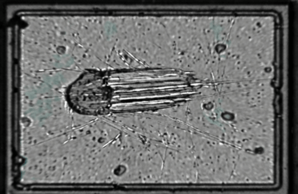
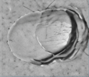
Conventional: Large Scrub Marks & Pad Damage (≤15µm)
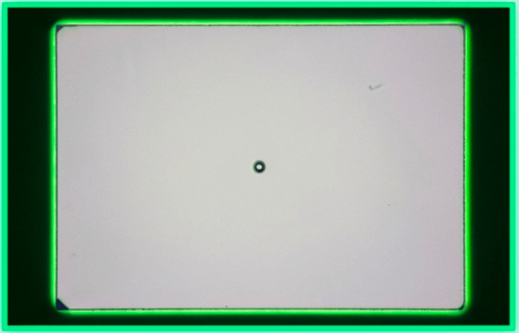
MEMS Type: Clean Contact, No Pad Damage (<4µm)
Radically reduces Gold Pad cost by reducing Pad Size.
Drastically reduces Gold Pad cost by reducing Pad Size.
6 Innovative Benefits of MEMS Vertical Probe Card
Cost Reduction
Pad size reduced from 40x80µm to 7x7µm.
Extended Lifespan
Life time increased from 500K to 1M cycles.
Faster Repair
70% reduction in repair time (2–3 days).
Improved Contact
Stable resistance due to reduced scrub marks.
Ultra-fine Pitch
Supports 27µm stacked fabrication.
Para Scalability
Multi-para production up to 526Para F/T.
Testing Parameter: @ 75µm OT
Extreme Durability Under Harsh Conditions
Average Force: 1.32gf
"Zero force degradation even after 13.1 million extreme repetitive tests."
The Birth of Next-Gen Innovation: VLWST Solution
Breaking the limits of high cost and long lead times to set new standards.
Reliant on imports, high unit price, and 5+ weeks lead time.
Exclusive VLWST Development
Success after 5 years of R&D and field tests with global fabless leaders.
Drastic cost reduction and lead time shortened to within 3 weeks.
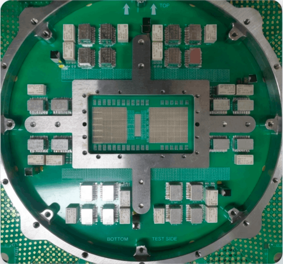
A Difference That Changes the Paradigm
How TESTONIC VLWST outperforms conventional Japanese MLC technology.
Secret of Technical Superiority: Internal Optimization
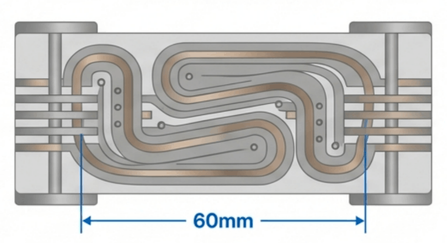
Conventional MLC: 60mm Pattern Length (High signal loss due to long path).
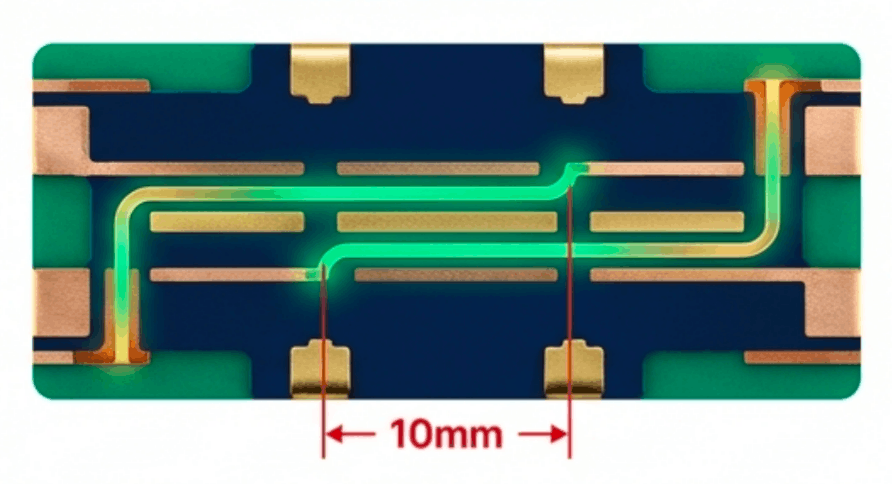
Innovative VLWST: 10mm Pattern Length (Ultra-fast transmission via short path).
Internal pattern length reduced by 1/6, achieving overwhelming speed characteristics of ≥3.2GHz.